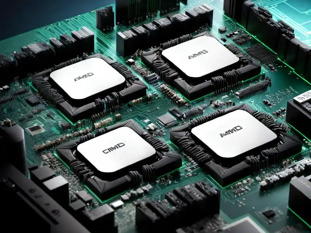
What are Chiplets?
Chiplets are small, modular dies that contain specific CPU components like cores, cache, and I/O. Instead of making an entire CPU on one large die, chipmakers can connect multiple chiplets together to create a complete CPU package.
This allows AMD and other chipmakers to:
- Mix and match chiplets with different combinations of cores, cache, etc.
- Improve yields since smaller dies have fewer defects.
- Enable chiplet reuse across products.
- Achieve modular designs by upgrading or swapping chiplets.
Why AMD Adopted Chiplets
AMD first introduced their chiplet architecture with their 7nm Zen 2 CPUs in 2019. There were several reasons AMD made this radical shift:
- Overcome manufacturing limitations of large, monolithic dies at 7nm and beyond.
- Improve scalability by mixing chiplets with different core counts.
- Increase flexibility to create CPUs for everything from laptops to data centers.
- Reduce costs by improving yields and reusing chiplets across products.
AMD’s Chiplet Design
AMD packages together several different chiplets to create their Ryzen desktop CPUs and EPYC server CPUs:
CCD Chiplets
- Contains Zen CPU cores, L3 cache.
- Available with up to 8 cores per chiplet.
- Mix and match to scale core count.
I/O Die
- Handles memory controllers, PCIe lanes, Infinity Fabric.
- Produced on older manufacturing process for higher yields.
Additional Chiplets
- GPU chiplets on APUs like Ryzen 6000.
- V-Cache chiplets stacking L3 cache on some models.
This modular design allows AMD to scale products from 6 cores for mobile up to 64 cores for servers.
Benefits of Chiplets
Adopting small, reusable chiplets provides AMD several advantages over large monolithic dies:
- Lower manufacturing costs – Improved yields with smaller dies.
- Flexibility – Mix and match chiplets for different markets.
- Scalability – Easily scale core counts and cache.
- Performance – Overcome reticle limits of large dies.
- Time-to-market – Reuse existing chiplets in new products.
The Future of Chiplets
AMD’s chiplet architecture has been a huge success so far. The company is investing heavily to take their chiplet strategy further:
- Enhanced chiplet interconnects – Improve bandwidth and latency between chiplets.
- 3D stacking – Stack chiplets vertically to increase density.
- Chiplet reuse – Continue reusing chiplets across generations.
- Heterogeneous integration – Combine different process nodes and architectures.
- Chiplet standardization – Allow 3rd party chiplets in CPUs.
Challenges for Chiplet Adoption
While promising, chiplet architectures also come with some challenges:
- Added complexity of splitting dies.
- Potential yield and binning challenges.
- Extra power consumption from chiplet interconnects.
- Thermal density challenges with 2.5D and 3D packaging.
- Need to design the entire system, not just individual chiplets.
Conclusion
AMD’s innovative chiplet architecture represents the future of CPU design in the post-Moore’s Law era. By mixing small modular chiplets, AMD can overcome limitations of large dies and achieve new levels of flexibility, performance and efficiency. While not without challenges, chiplets provide the most scalable path forward as process nodes continue to slow down. With their head start on chiplet design, AMD is positioned as a leader in next-generation CPU architectures.


